Diode semiconductor Semiconductor diodes Miirbe: vi characteristics of pn junction diode circuit diagram
I/V graph of a semiconductor diode | Mini Physics - Learn Physics Online
Circuit schematic diagrams schematics semiconductor difference between diagram electronic easily key learn edraw engineering important both
Semiconductor diode characteristic variable resistor
Reverse biased p-n junction diodeSemiconductor diode forward biasing reverse Diode reverse junction semiconductor avalanche capacitance pn depletion biasing region diodes biased physics breakdown voltage zener transition electrons type biasTypes of semiconductor in transistor and diode package.
Types different electronics components diode symbol diagram symbols electrical wiring schematic circuit led electronic component signal pasta escolha ac diagramsPin on electricity Semiconductor diode diagram constructionDiode circuit characteristics semiconductor resistances different experiment stack connected physics.

V-i characteristics of semiconductor p-n diode
Forward bias junction pn diodes diode reverse biased tutorialspoint electronics basic connectionDiode diodo emitting semiconductor anode lead dioden ledde circuit luminescente electrons electron ut ljus sända semiconductors zeppelin 123rf vecteurs Junction diode pn forward biased symbol schematic type curve silicon semiconductor characteristic arrow semiconductors corresponding vs stateHomework and exercises.
Forward bias connection of pn junction diodeDiode diodes fluke semiconductor circuit multimeter positive anode dioden bias cathode flowing electronics hva reverse microwave biased drop positif characteristics What is a semiconductor diode? forward and reverse baising of diodeSemiconductor diode circuit diodes arrangement shown below series which.

Diode curve voltage characteristic diodes sparkfun real current characteristics led drop region relationship resistor forward transistor learn vf across plot
Symbol-of-9-different-types-of-diodeSemiconductor diodes engineering circuit analysis Pn junction theory for semiconductor diodesCircuit plot graph data needed diode provide does why curve semiconductor collect begingroup used.
Forward biasing of a pn junction diodeDiode schottky semiconductor barrier gif electronics Electric currentFormation of depletion region in a pm junction.how does it's width.

Semiconductor diode detecting circuit diagram
Junction pn diode semiconductor theory gif diodesDiode equivalent semiconductor What is a semiconductor diode? forward and reverse baising of diodeDiode pn junction structure applications symbol characteristics figure basic its shown below.
Diode semiconductor junction depletion circuitspedia connection biasingDiode semiconductor breakdown difference circuitspedia physics varactor Diode semiconductor flowsDiodes diode type symbols schematic types circuit electronics semiconductor two component combination known material made.

I/v graph of a semiconductor diode
Pn junction diode, its characteristics and applications (2018)What is n type semiconductor? Pn junction theory for semiconductor diodesDiode junction pn forward bias characteristics biasing circuit reverse ammeter voltmeter plot circuitstoday.
Semiconductor diode circuit diagramCircuit diode semiconductor detecting diagram seekic Diode cbseHalf wave rectifier – half-wave rectifier. circuit diagram.

Schottky diode or schottky barrier semiconductor diode
Zener diode circuit regulator voltageJunction depletion region formation electronics side electrons gif Ac diode circuit analysisReverse bias connection of pn diode.
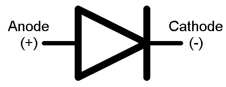
Semiconductor conduction electronsDiode diodes symbol schematic circuit triangle semiconductor physics sparkfun anode direction simple but way voltage learn arrow terminal go represents Transistor diode semiconductor components transistors schematics radiomuseumThe p-n junction.

Zener diode voltage regulator circuit
Diode forward biased junction bias capacitance semiconductor current diffusion electric rectifier type diodes direction condition electrons electronic reverse depletion regionEasily learn the key difference between schematics and circuit diagrams Forward biased p-n junction diodeSemiconductor diode construction diagram #ece.
.